 | –≠–Ľ–Ķ–ļ—ā—Ä–ĺ–Ĺ–Ĺ—č–Ļ –ļ–ĺ–ľ–Ņ–ĺ–Ĺ–Ķ–Ĺ—ā: THAT4311 | –°–ļ–į—á–į—ā—Ć:  PDF PDF  ZIP ZIP |
THAT Corporation; 45 Sumner Street; Milford, Massachusetts 01757-1656; USA
Tel: +1 508 478 9200; Fax: +1 508 478 0990; Web: www.thatcorp.com
THAT 4311
Description
The THAT 4311 Low Power Dynamics Proces-
sor combines in a single IC all the active circuitry
needed to construct a wide range of dynamics
processors.
The 4311 includes a high perfor-
mance, voltage controlled amplifier, a log re-
sponding RMS-level sensor and three opamps,
one of which is dedicated to the VCA, while the
other two may be used for the signal path or con-
trol voltage processing.
The exponentially-controlled VCA provides
two opposing-polarity, voltage sensitive control
ports. Dynamic range exceeds 105 dB, and THD
is typically 0.09% at 0dB gain. The RMS detector
provides accurate RMS to DC conversion over an
80 dB dynamic range.
Though originally designed for use in micro-
phone noise reduction systems, the 4311 is a use-
ful building block in a number of analog signal
processing applications. The combination of ex-
ponential VCA gain control and logarithmic detec-
tor
response
-
"decibel-linear"
response
-
simplifies the mathematics of designing the con-
trol paths of dynamics processors, making it easy
to develop audio compressors, limiters, gates, ex-
panders, de-essers, duckers, and the like.
The
high level of integration ensures excellent temper-
ature tracking between the VCA and the detector,
while minimizing the external parts count.
T H A T
C o r p o r a t i o n
Low-voltage, Low-power
Analog Engine
ģ
Dynamics Processor
FEATURES
∑
High Performance VCA, RMS-Level
Detector, and three 0pamps in one
package
∑
Wide Dynamic Range: >105 dB
∑
Low THD: <0.09%
∑
Low Power: 7 mA typ.
∑
Surface-Mount Package
∑
5 VDC Operation
APPLICATIONS
∑
Wireless microphone systems
∑
Wireless in-ear monitors
∑
Compressors and Limiters
∑
Gates
∑
De-Essers
∑
Duckers
18
19
20
17
16
15
14
13
12
11
7
9
8
6
10
5
4
3
2
1
THAT4311
VREF
OA1
OA2
VEE
EC-
EC+
SYM
IN
OUT
IN
CT
OUT
IT
VCA
RMS
OA3
VCC
VREF
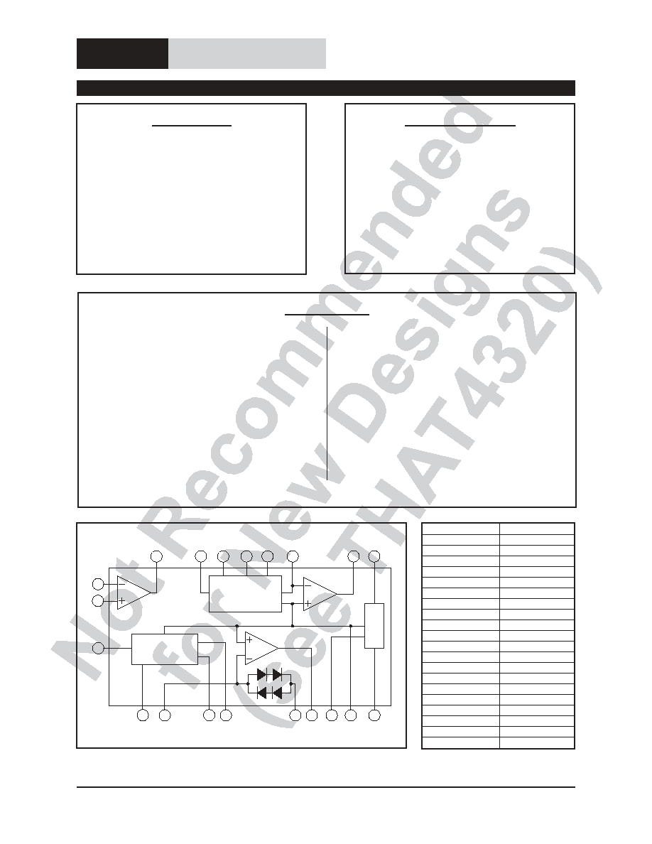
Figure 1. THAT 4311 equivalent block diagram
Pin Name
DMP20
RMS IN
1
IT (I
TIME
)
2
OA2 -IN
3
RMS OUT
4
CT (C
TIME
)
5
CLIP
6
OA2 OUT
7
CAP
8
VREF
9
VEE
10
VCC
11
OA3 OUT
12
VCA OUT
13
SYM
14
EC+
15
EC-
16
VCA IN
17
OA1 OUT
18
OA1 -IN
19
OA1 +IN
20
Table 1. THAT 4311 pin assignments

THAT Corporation; 45 Sumner Street; Milford, Massachusetts 01757-1656; USA
Tel: +1 508 478 9200; Fax: +1 508 478 0990; Web: www.thatcorp.com
Page 2
Low-voltage, Low-power Analog Engine
ģ
Dynamics Processor
Absolute Maximum Ratings (T
A
= 25įC)
Positive Supply Voltage (V
CC
)
+15 V
Power Dissipation (P
D
) (T
A
= 75įC)
700 mW
Operating Temperature Range (T
OP
)
-20 to +70įC
Storage Temperature Range (T
ST
)
-40 to +125įC
Max
DE
C
E
C+
- (E
C-
)
Ī 1V
Electrical Characteristics
2
Parameter
Symbol
Conditions
Min
Typ
Max
Units
Supply Current
I
CC
No signal; V
CC
=+7 VDC
--
7.0
9.0
mA
Reference Voltage
V
REF
1.8
1.95
2.1
V
Encode and Decode ≠ Companding Noise Reduction ( V
CC
= +7V encoder, +15V decoder)
Encode Level Match
LMe
Encode mode; f = 1kHz
-25.3
-23.0
-20.7
dBV
Encode Gain Accuracy
Encode mode, f = 1kHz
GAe1
Vin = LMe + 10dB
+3.5
+5
+6.5
dB
GAe2
Vin = LMe - 40dB
-23
-20
-17
dB
Decode Level Match
LMd
Decode mode; f = 1kHz
-18.3
-16.0
-13.7
dB
Decode Gain Accuracy
Decode mode; f=1kHz
GAd1
Vin = LMd + 5dB
+8.5
+10
+11.5
dB
GAd2
Vin = LMd - 20dB
-43
-40
-37
dB
Max Input Voltage
Vime
Encode mode; THD = 3%; f = 1kHz
3
5
--
dBV
Max Output Voltage
Vomd
Decode mode; THD = 3%; f = 1kHz
10.7
13.7
--
dBV
Total Harmonic Distortion
THDtrim
End-to-end; Vin = LMe; f = 1kHz
--
0.025
--
%
(with trim)
Total Harmonic Distortion
THDnotrim
End-to-end; Vin = LMd; f = 1kHz
--
0.15
0.7
%
(no trim)
Output Noise
Vnod
End-to-end ; Vin = short; A-weighted
--
7
--
ĶVrms
Recommended Operating Conditions
Parameter
Symbol
Conditions
Min
Typ
Max
Units
Positive Supply Voltage
V
CC
+5
+15
V
SPECIFICATIONS
1
1. All specifications are subject to change without notice.
2. Unless otherwise noted, T
A
=25įC, test circuit as shown in Fig 2.
THAT Corporation; 45 Sumner Street; Milford, Massachusetts 01757-1656; USA
Tel: +1 508 478 9200; Fax: +1 508 478 0990; Web: www.thatcorp.com
Rev. 03/03/04
Page 3
Electrical Characteristics (con't)
Parameter
Symbol
Conditions
Min
Typ
Max
Units
Op amp OA1
Offset Voltage
V
IO
RL = 2k
W
--
Ī0.5
Ī6
mV
Equivalent Input Noise
V
nOA1
A-weighted
6.5
10
nV
Hz
Total Harmonic Distortion
THD
OA1
1kHz, A
V
=1; R
L
= 10k
W
--
0.0007
0.003
%
Open Loop Gain
A
VO-OA1
R
L
= 10k
W
--
115
--
Gain Bandwidth Product
GBW
OA1
at 50kHz
--
5
--
Slew Rate
SR
OA1
--
2
--
Op amp OA2
Offset Voltage
V
IO
RL = 2k
W
--
Ī0.5
Ī6
mV
Equivalent Input Noise
V
nOA1
A-weighted
7.5
12
nV
Hz
Total Harmonic Distortion
THD
OA1
1kHz, A
V
=1; R
L
= 10k
W
--
0.0007
0.003
%
Open Loop Gain
A
VO-OA1
R
L
= 10k
W
--
110
--
Gain Bandwidth Product
GBW
OA1
at 50kHz
--
5
--
Slew Rate
SR
OA1
--
2
--
R11
23k2
R14
31k6
R22
30R1
R16
280R
C6
47u
V-
R12
261k
R9
51R
5%
R8
300k 5%
R6
20k0
C5
47p NPO
R5
20k0
C4
47u
R7
50k
Sym
cw
V+
R10
100R 5%
C7
10u
R26
100R
5%
TP2
RMS Output
TP1
RMS Input
R17
31k6
C8 47p
R20
10k0
R21
10k0
C9
3u3
1
2
3
CN1
External
Control
Input
CONTROL-VOLTAGE
1
2
3
CN2
Power
Input
C11
100n
(U1)
C10
22u
V+
Bypass
Capacitors
XLR2
XLR-M
Output
C17
47p
D3
1N4004
IN
17
14
15
13
12
16
OUT
VCA
EC+
SYM
EC-
OA3
VREF
U1A
THAT4311
Iset
2
TC
5
IN
1
OUT 4
RMS
U1B
THAT4311
3
7
OA2
VREF
6
U1C
THAT4311
18
19
20 OA1
U1D
THAT4311
CAP
8
VEE
10
VREF
9
VCC
11
VREF
U1E
THAT4311
3
2
6
8
1
U1
OP-27
R1
100k
R4
1k33
R3
10k0
R29
1k33 VREF
R23
280R
R24
2k80
C15
1000u
C16
47u
R27
10k0
R18
10k0
R19
100k
V+
R15
31k6
C19
1000u
C2
10u
C3
22u
C1
10u
V+
VREF
R2
10k0
C12
3u3
+40dB
+20dB
+40dB
+60dB
C18
47u
2
15
SW1B
5
12
SW1E
6
11
SW1F
C14
100n
(U1)
C13
22u
D4
1N4004
V-
V-
VREF
R25
100R
5%
R28
100R 5%
1
16
SW1C
SW1A
1
2
3
CN1
RMS Output
VREF
0dB
5 4
3 1
2
2
3
1
XLR1
XLR-F
Input
5
4
3
1
2
2
3
1
+
+
+
+
+
+
+
+
+
+
+
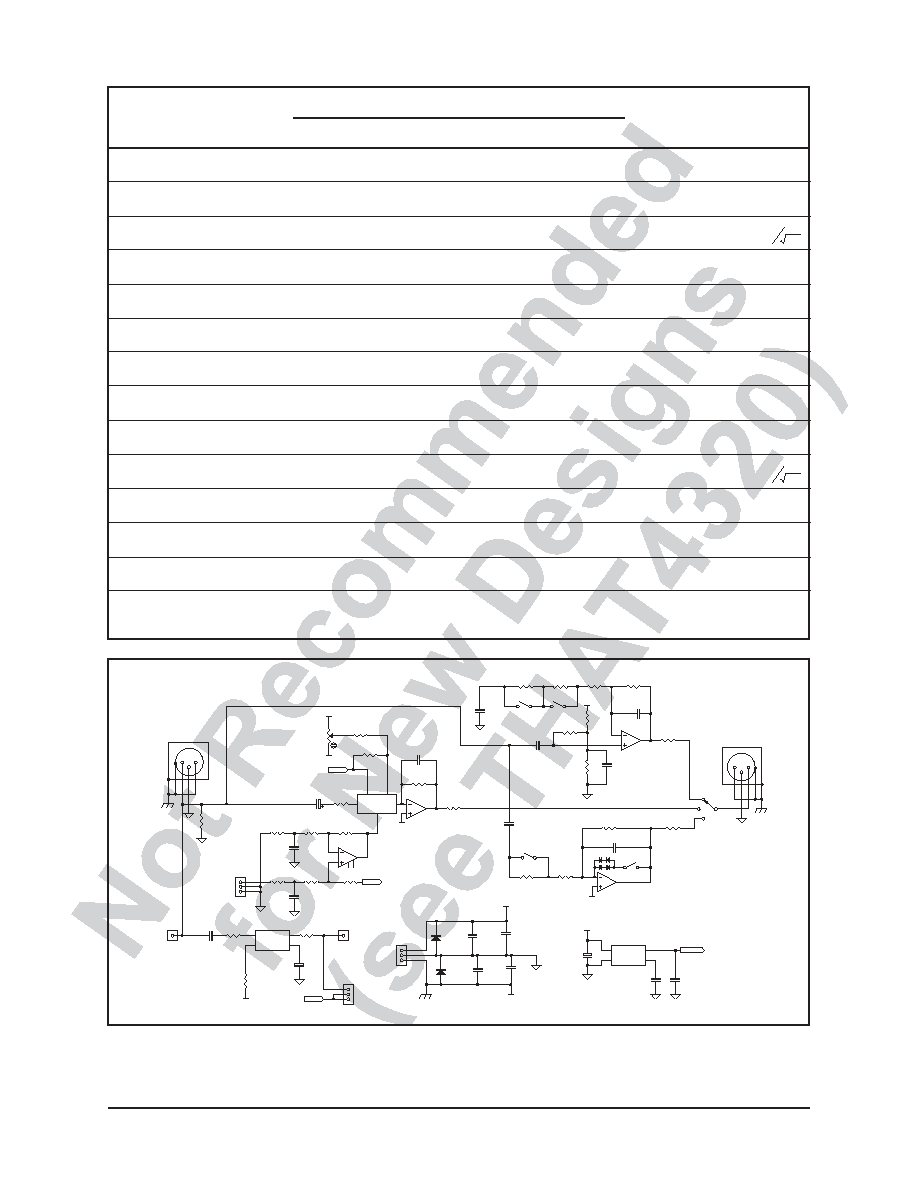
Fig 2. THAT 4311 test circuit
Representative Data (Stand-alone)
THAT Corporation; 45 Sumner Street; Milford, Massachusetts 01757-1656; USA
Tel: +1 508 478 9200; Fax: +1 508 478 0990; Web: www.thatcorp.com
Page 4
Low-voltage, Low-power Analog Engine
ģ
Dynamics Processor
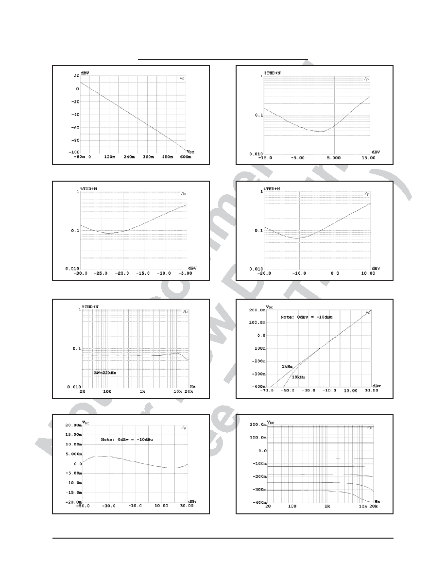
Fig 3. VCA Gain vs. Control Voltage (Ec-) at 25
įC
Fig 4. VCA 1kHz THD+Noise vs. Input, -15 dB Gain
Fig 5. VCA 1kHz THD+Noise vs. Input, +15 dB Gain
Fig 6. VCA 1kHz THD+Noise vs. Input, 0 dB Gain
Fig 7. VCA THD vs. Frequency, 0 dB gain, 1 Vrms Input
Fig 9. Departure from Ideal Detector Law vs. Level
Fig 8. RMS Output vs. Input Level, 1 kHz & 10 kHz
Fig 10. Detector Output vs. Frequency at Various Levels
Representative Data (Companding Noise Reduction)
THAT Corporation; 45 Sumner Street; Milford, Massachusetts 01757-1656; USA
Tel: +1 508 478 9200; Fax: +1 508 478 0990; Web: www.thatcorp.com
Rev. 03/03/04
Page 5
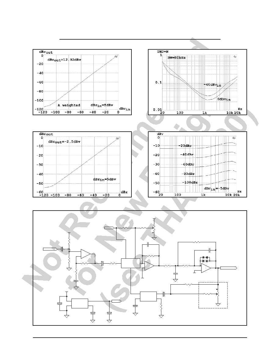
Fig 11. End-to-End Transfer Function, 1kHz
Fig 12. End-to-End THD+N
Fig 13. Encoder Transfer Function, 1kHz
Fig 14. Encoder Frequency Response 20-20kHz
IN
17
12
OUT
VCA
EC+
SYM
EC-
OA3
Vref
U1A
THAT4311
Iset
2
TC
5
IN
1
OUT
4
RMS
U1B
THAT4311
3
7
OA2
Vref
6
U1C
THAT4311
18
19
20
U1D
THAT4311
R1
200k
R2
200k
R13
2k
R3
8k06
R5
15k
R9
51R
R8
50k
R6
30k
R11B
10k
R12
261k
C1
10n
C5
270p
C4
3u3
C7
10u
R7
20k
C6
10u
V+
C3
10u
C8
22u
V+
+5
C2
3u3
Encoder
In
Vref
Vref
22kHz 3 pole BW filter
Cap
8
Vee
10
Vref
9
Vcc
11
Vref
U1E
THAT4311
R4
6k19
R10
6k19
C9
570p
Encoder
Out
C16
10u
R31
4k32
C10
4n7
VR1
20k
R11A
20k
optional
15
14
13
16
+
+
+
+
+
+
+
+
_
+
_
_
_
+
Fig 15. THAT 4311 Noise Reduction Encoder Schematic
THAT Corporation; 45 Sumner Street; Milford, Massachusetts 01757-1656; USA
Tel: +1 508 478 9200; Fax: +1 508 478 0990; Web: www.thatcorp.com
Page 6
Low-voltage, Low-power Analog Engine
ģ
Dynamics Processor
Theory of Operation
The THAT 4311 Analog Engine‚ Dynamics Pro-
cessor combines THAT,s proven Voltage-Controlled
Amplifier (VCA) and RMS-Level Detector designs with
three opamps to produce a multipurpose dynamics
processor useful in a variety of applications. For de-
tails of the theory of operation of the VCA and RMS
Detector building blocks, the interested reader is re-
ferred to THAT Corporation's data sheets on the
218x Series VCAs and the 2252 RMS-Level Detector.
Theory
of
the
interconnection
of
exponen-
tially-controlled VCAs and log-responding level detec-
tors is covered in THAT Corporation's application
note AN101, The Mathematics of Log-Based Dynamic
Processors.
The VCA - in Brief
The THAT 4311 VCA is based on THAT Corpora-
tion's highly successful complementary log/anti-log
gain cell topology, as used in THAT's 218x and
215x-Series IC VCAs. The THAT 4311 is integrated
using a fully complementary, BiFET process.
The
combination of FETs with high-quality, complemen-
tary bipolar transistors (NPNs and PNPS) allows ad-
ditional flexibility in the design of the VCA over
previous efforts.
Input signals are currents to the VCA IN pin.
This pin is a virtual ground biased at VREF, so in
normal operation an input voltage is converted to in-
put current via an appropriately sized resistor (R5 in
Fig 2, Page 3). Because the current associated with
DC offsets relative to VREF present at the input pin
and any DC offset in preceding stages will be modu-
lated by gain changes (thereby becoming audible as
thumps), the input pin is normally AC-coupled (C4 in
Fig 2).
The VCA output signal is also a current, inverted
with respect to the input current. In normal opera-
tion, the output current is converted to a voltage via
inverter OA3, where the ratio of the conversion is de-
termined by the feedback resistor (R6, Fig 2) con-
nected between OA3's output and its inverting input.
The signal path through the VCA and OA3 is
non-inverting.
The gain of the VCA is controlled by the voltage
applied between EC- and the combination of EC+
and SYM. Gain (in decibels) is proportional to EC-,
provided that EC+ and SYM are at VREF. The con-
stant of proportionality is -6.1mV/dB (for 5V sup-
plies) for the voltage at EC-, and 6.1mV/dB for the
voltage at EC+, and SYM
IN
12
OUT
VCA
EC+
SYM
EC-
OA3
Vref
U1A
THAT4311
Iset
2
TC
5
IN
1
OUT
4
RMS
U1B
THAT4311
Cap
8
Vee
10
Vref
9
Vcc
11
Vref
U1E
THAT4311
R5
24k3
R9
51R
R8
150k
R6
24k3
R11
15k
R12
261k
C1
3n3
C4
3u3
C5
10u
R7
20k
C6
10u
V+
C2
10u
C3
22u
Decoder In
Decoder Out
R1
6k04
+15
R2
56k
R3
8k87
C16
10u
18
19
20
OA1
U1D
THAT4311
R4
7k5
C7
10u
13
14
15
16
17
+
+
+
+
+
+
+
+
+
_
_
Fig 16. THAT 4311 Noise Reduction Decoder Schematic
THAT Corporation; 45 Sumner Street; Milford, Massachusetts 01757-1656; USA
Tel: +1 508 478 9200; Fax: +1 508 478 0990; Web: www.thatcorp.com
Rev. 03/03/04
Page 7
As mentioned, for proper operation, the same
voltage must be applied to EC+ and SYM, except for
a small (Ī2.5 mV) DC bias applied between these
pins.
This bias voltage adjusts for internal mis-
matches in the VCA gain cell which would otherwise
cause small differences between the gain of positive
and negative half-cycles of the signal. The voltage is
usually applied via an external trim potentiometer
(R7 in Fig 2), which is adjusted for minimum signal
distortion at unity (zero dB) gain.
The VCA may be controlled via EC-, as shown in
Fig 17, or via the combination of EC+ and SYM.
This connection is illustrated in Fig 18.
Note that
this latter figure shows only that portion of the cir-
cuitry needed to drive the positive VCA control port;
circuitry associated with OA1, OA2 and the RMS de-
tector has been omitted.
While the 4311's VCA circuitry is very similar to
that of the THAT 2180 Series VCAs, there are several
important differences, as follows:
1. Supply current for the VCA is fixed internally.
Approximately 500
mA is available for the sum of in-
put and output signal currents.
2. The signal current output of the VCA is inter-
nally connected to the inverting input of an on-chip
opamp.
In order to provide external feedback
around this opamp, this node is brought out to a pin.
3. The input stage of the 4311 VCA uses inte-
grated P-channel FETs rather than a bias-current
corrected bipolar differential amplifier.
Input bias
currents have therefore been reduced.
The RMS Detector - in Brief
The THAT 4311's detector computes RMS level
by rectifying input current signals, converting the rec-
tified current to a logarithmic voltage, and applying
that voltage to a log-domain filter. The output signal
is a DC voltage proportional to the decibel-level of the
RMS value of the input signal current.
Some AC
component (at twice the input frequency) remains su-
perimposed on the DC output. The AC signal is at-
tenuated by a log-domain filter, which constitutes a
single-pole roll-off with cutoff determined by an ex-
ternal capacitor and a programmable DC current.
As in the VCA, input signals are currents to the
RMS IN pin. This input is a virtual ground biased at
VREF, so a resistor (R11 in Fig 2) is normally used to
convert input voltages to the desired current.
The
level detector is capable of accurately resolving sig-
nals well below 10mV (with a 10k
W input resistor).
However, if the detector is to accurately track such
low-level signals, AC coupling is normally required.
IN
17
12
OUT
VCA
EC+
SYM
EC-
OA3
Vref
U1A
THAT 4311
Iset
2
TC
5
IN
1
OUT
4
RMS
U1B
THAT 4311
3
7
OA2
Vref
6
U1C
THAT 4311
18
19
20
OA1
U1D
THAT 4311
Cap
8
Vee
10
Vref
9
Vcc
11
Vref
U1E
THAT 4311
Vref
Vref
R1
20k
R2
20k
R3
51R
R4
51k
R6
10k
R7
264k
C1
47u
C2
47p
C3
47u
C4
10u
C5
10u
C8
22u
C7
100n
R5
20k
+5
+5
Signal In
RMS Out
Signal Out
C6
10u
Control Port Drive
15
14
13
16
+
+
+
+
+
+
Fig 17. Circuit showing gain control at E
C-
THAT Corporation; 45 Sumner Street; Milford, Massachusetts 01757-1656; USA
Tel: +1 508 478 9200; Fax: +1 508 478 0990; Web: www.thatcorp.com
Page 8
Low-voltage, Low-power Analog Engine
ģ
Dynamics Processor
The log-domain filter cutoff frequency is usually
placed well below the frequency range of interest.
For an audio-band detector, a typical value would be
5Hz, or a 32ms time constant (
t). The filter's time
constant is determined by an external capacitor at-
tached to the CT pin, and an internal current source
(I
TIME
) connected to CT. The current source is pro-
grammed via the IT pin: current in IT is mirrored to
I
TIME
with a gain of approximately one. The resulting
time
constant
t is approximately equal to
(0.026
ī CT) / I
T
. Note that, as a result of the mathe-
matics of rms detection, the attack and release time
constants are fixed in their relationship to each other.
The DC output of the detector is scaled with the
same constant of proportionality as the VCA gain
control: 6.1mV/dB. The detector's zero dB reference
(Iin0, the input current which causes zero volts out-
put), is determined by IT as follows:
Iin0=IT. The
detector output stage is capable of sinking or sour-
cing l00
mA.
Differences between the 4311's RMS-Level Detec-
tor circuitry and that of the THAT 2252 RMS Detec-
tor are as follows:
1. The rectifier in the 4311 RMS Detector is inter-
nally balanced by design, and cannot be balanced via
an external control. The 4311 will typically balance
positive and negative halves of the input signal within
Ī1.5%, but in extreme cases the mismatch may
reach +20%. However, a 20% mismatch will not sig-
nificantly increase ripple-induced distortion in dy-
namics processors over that caused by signal ripple
alone.
2. The time constant of the 4311's RMS detector
is determined by the combination of an external ca-
pacitor (connected to the CT pin) and an internal,
programmable current source. The current source is
equal to IT. Normally, a resistor is not connected di-
rectly to the CT pin on the 4311.
3. The zero dB reference point, or level match, is
not adjustable via an external current source. How-
ever, as in the 2252, the level match is affected by the
timing current, which, in this case, is drawn from the
IT pin and mirrored internally to CT.
4. The input stage of the 4311 RMS detector uses
integrated P-channel FETs rather than a bias-current
corrected bipolar differential amplifier.
Input bias
currents are therefore negligible, improving perfor-
mance at low signal levels.
The Opamps - in Brief
The three opamps in the 4311 are intended for
general purpose applications. All are 5MHz opamps
with slew rates of approximately 2V/
ms. All use bipo-
lar PNP input stages. However, the design of each is
optimized for its expected use. Therefore, to get the
IN
17
12
OUT
VCA
EC+
SYM
EC-
OA3
Vref
U1A
THAT 4311
Iset
2
TC
5
IN
1
OUT
4
RMS
U1B
THAT 4311
3
7
OA2
Vref
6
U1C
THAT 4311
18
19
20
OA1
U1D
THAT 4311
Cap
8
Vee
10
Vref 9
Vcc
11
Vref
U1E
THAT 4311
Vref
R1
20k
R2
20k
R3
51R
R4
51k
C1
47u
C2
47p
C5
10u
C8
22u
C7
100n
R5
50k
+5
+5
Signal In
Signal Out
Control Port Drive
N/C
N/C
N/C
N/C
N/C
N/C
N/C
N/C
N/C
15
14
13
16
+
+
+
Fig 18. Circuit showing gain control at E
C+
THAT Corporation; 45 Sumner Street; Milford, Massachusetts 01757-1656; USA
Tel: +1 508 478 9200; Fax: +1 508 478 0990; Web: www.thatcorp.com
Rev. 03/03/04
Page 9
most out of the 4311, it is useful to know the major
differences among these opamps.
OA3, being internally connected to the output of
the VCA. is intended for current-to-voltage conver-
sion.
Its input noise performance, at 7 5
.
/
nV
Hz,
complements that of the VCA, adding negligible noise
at unity gain. Its output section is capable of driving
1mA into a 2k
W load.
OA1 is the quietest opamp of the three, and with
its typical input referred noise of 6 5
.
/
nV
Hz, is the
opamp of choice for input stages. Its output section
is nominally capable of driving 3mA into a 5k
W load.
OA2 is best suited for control voltage processing,
though is does have anti-paralleled diodes that can
be used to fashion it into a clipper. (However in most
applications where a clipper is needed, it's preferable
to place it around OA3). OA2's input noise is compa-
rable to OA3 and its output drive is comparably to
OA1.
The Reference Voltage - In Brief
THAT Corporation's log/anti-log VCAs and RMS`
detectors require a reference voltage between the pos-
itive and negative power supplies, and to supply this,
the THAT 4311 provides an on-chip, 2V reference
about which the VCA, the RMS detector, and OA2 are
biased. This reference is a buffered band-gap refer-
ence that is amplified to 2V. Pins are provided for fil-
ter capacitors at both the input and the output of the
buffer, which are labeled CAP and VREF respectively.
Application Information
As noted previously, the THAT 4311 was origi-
nally designed for noise reduction systems, hence the
emphasis on those parameters in the specifications.
Its low power consumption, integration, and similar-
ity to the THAT 4301, however, extend its utility to a
variety of other products and applications. The cir-
cuit of Fig 19, shows a typical application for the
THAT 4311. This simple compressor/limiter design
features adjustable hard-knee threshold, compres-
sion ratio, and static gain. The applications discus-
sion in this data sheet will center on this circuit for
the purpose of illustrating important design issues.
Signal Path
As mentioned in the section on theory, the VCA
input pin is a virtual ground with negative feedback
provided internally. An input resistor (R1, 20k
W) is
required to convert the AC input voltage to a current
IN
17
12
OUT
VCA
EC+
SYM
EC-
OA3
Vref
U1A
THAT4311
Iset
2
TC
5
IN
1
OUT
4
RMS
U1B
THAT 4311
3
7
OA2
Vref
6
U1C
THAT4311
18
19
20
OA1
U1D
THAT4311
Cap
8
Vee
10
Vref
9
Vcc
11
Vref
U1E
THAT 4311
R1
20k
R2
20k
R3
51R
R4
33k
R5
20k
R15
10k
R6
28k7
R7
267k
R8
4k99
R9
10k
R10
82k
R12
20k
R13
10k
R11
51k
R17
82k
R16
4k99
R14
1k43
R18
50k
C1
47u
C2
47p
C3
47u
C4
10u
C5
100n
C7
100n
C8
10u
C9
22u
Vref
Vref
Vref
+5
+5
+5
+5
C6
10u
In
Out
Vin0=-10dBu
CR1
1N4148
CR2
1N4148
Gain
Threshold
Compression
Ratio
15
14
13
16
+
+
+
+
+
+
Fig 19. Simple compressor / limiter using the THAT 4311

THAT Corporation; 45 Sumner Street; Milford, Massachusetts 01757-1656; USA
Tel: +1 508 478 9200; Fax: +1 508 478 0990; Web: www.thatcorp.com
Page 10
Low-voltage, Low-power Analog Engine
ģ
Dynamics Processor
within the linear range of the THAT 4311. (Peak VCA
input currents should be kept under 250
mA for best
distortion performance.) The coupling capacitor (Cl,
47
mF) is strongly recommended to block DC current
from preceding stages (and from offset voltage at the
input of the VCA). Any DC current into the VCA will
be modulated by varying gain in the VCA, showing up
in the output as "thumps". Note that Cl, in conjunc-
tion with R1, will set the low frequency limit of the
circuit.
The VCA output is connected to OA3, configured
as an inverting current-to-voltage converter.
OA3's
feedback components (R2, 20 k
W, and C2, 47 pF) de-
termine the constant of current-to-voltage conversion.
The simplest way to deal with this is to recognize that
when the VCA is set for unity (zero dB) gain, the in-
put to output voltage gain is simply R2/R1, much like
the case of a single inverting stage. If, for some rea-
son, more than zero dB gain is required when the
VCA is set to unity, then the resistors may be skewed
to provide it. Note that the feedback capacitor (C2) is
required for stability. The VCA output has approxi-
mately 45pF of capacitance to ground, which must be
neutralized via the 47pF feedback capacitor across
R2.
The VCA gain is controlled via the EC- terminal,
whereby gain in dB will be proportional to the nega-
tive of the voltage at EC-. In this application the EC+
terminal is tied to VREF, though it could be the
driven port, or the control ports could be driven dif-
ferentially. The SYM terminal is returned nearly to
the EC+ terminal (which is in this case VREF) via a
small resistor (R3, 51
W). The VCA SYM trim (R5,
20k
W) allows a small voltage to be applied to the
SYM terminal via R4 (33k
W). This voltage adjusts for
small mismatches within the VCA gain cell, thereby
reducing even-order distortion products.
To adjust
the trim, apply to the input a middle-level, mid-
dle-frequency signal (1kHz at 200mV
rms
is a good
choice with this circuit) and observe THD at the sig-
nal output. Adjust the trim for minimum THD.
RMS-Level Detector
The RMS detector's input is similar to that of the
VCA. An input resistor (R6, 28.7k
W) converts the AC
input voltage to a current within the linear range of
the THAT 4311. The coupling capacitor (C3, 47
mF)
is recommended to block the current from preceding
stages (and from offset voltage at the input of the de-
tector). Any DC current into the detector will limit
the low-level resolution of the detector, and will upset
the rectifier balance at low levels. Note that, as with
the VCA input circuitry, C3 in conjunction with R6
will set the lower frequency limit of the detector.
The time response of the RMS detector is deter-
mined by the capacitor attached to CT (C4, 10 uF)
and the size of the current in pin IT (determined by
R7, 267 k
W and VREF, 2V). Since the voltage at IT is
approximately 2V, the circuit of Figure 19 produces
7.5
mA in IT, The current in IT is mirrored to the CT
pin, where it is available to discharge the timing ca-
pacitor (C4). The combination produces a log filter
with time constant equal to approximately 0.026
CT/IT (~35 ms in the circuit shown).
The waveform at CT will follow the logged (deci-
bel) value of the input signal envelope, plus a DC off-
set of about 2V
BE
plus VREF or about 3.3V.
The
capacitor used should be a low-leakage, electrolytic
type in order not to add significantly to the timing
current.
The output stage of the RMS detector serves to
buffer the voltage at CT and removes the 1.3 V
DC
(2 V
BE
) offset, resulting in an output centered around
VREF for input signals of about 245 mV
rms
, or
-10 dBu. The output voltage increases 6.1 mV for ev-
ery 1 dB increase in input signal level. This relation-
ship holds over more than a 60 dB range in input
currents.
Control Path
The primary function of an audio compressor is
to reduce a signal's dynamic range. A 2:1 compres-
sor reduces a 100 dB dynamic range to 50 dB.
A
limiter, or infinite compressor, is a special case of
compressor where the dynamic range is reduced to
the point where the rms level of the signal is con-
stant.
This reduction in dynamic range is accom-
plished by a) raising the gain when the signal is
below some particular level -- often referred to as the
'zero dB reference level' -- and b) reducing the gain
when the signal is above that level. In addition, these
devices often have a threshold, below which the sig-
nal is passed unprocessed and above which compres-
sion takes place. This feature keeps the noise floor
from rising to noticeable levels in the absence of sig-
nal.
We previously established that the zero dB refer-
ence level of the detector is -10 dBu (zero dB refer-
ence level = 7.5
mA , R6 = 28.7 kilohms). Neglecting
the effect of the threshold control (R11 and R12),
when the output is below this level the output of OA2
is driven high, forward biasing CR1 and reverse bias-
ing CR2. Since CR2 is not conducting, no signal is
passed to the VCA's control port by OA1. When the
signal level exceeds -10 dBu, the output of the RMS
detector goes positive, and CR2 begins to conduct. In

THAT Corporation; 45 Sumner Street; Milford, Massachusetts 01757-1656; USA
Tel: +1 508 478 9200; Fax: +1 508 478 0990; Web: www.thatcorp.com
Rev. 03/03/04
Page 11
this case, OA2's feedback is provided through R9,
and the sensitivity at this point is 12.2 mV/dB, since
the output of the RMS detector is multiplied by
-R9/R8, or a gain of -2.
A threshold control is provided to vary the
threshold above or below -10 dBu. The output sensi-
tivity of the RMS detector is 6.1 mV/dB. This is con-
verted to a current by R8, and the sensitivity at the
summing node of OA2 is
6 1
4 99
12
.
.
.
mV
dB
k
A
W
=
m
The wiper of R12 can swing between -2V and +3V
relative to the summing node of OA2 which is at
VREF. If we want the threshold to swing as high as
+30 dB, then the value required for R11 can be cal-
culated as
R
k
V
dB
A
dB
11
51
2
1 2
30
=
Ľ
ī
.
m
W
when rounded to the nearest 5% resistor value.
Using this value and knowing that the pot's swing in
the other direction is 3V, we can calculate the thresh-
old swing in the negative direction to be
3
51
1 2
49
V
k
A
dB
dB
W
.
m
Ľ -
Since the zero dB reference level of the detector is
-10 dBu, the threshold can be adjusted from 20 dBu
to -59 dBu.
The output of the threshold detector represents
the signal level above the determined threshold, at a
constant
of
about
13mV/dB
(from
[R9/R8]
6.1mV/dB).
This signal is passed on to the COM-
PRESSION control (R13), which variably attenuates
the signal passed on to OA1. Note that the gain of
OA1, from the wiper of the COMPRESSION control to
OA1's output is R16/R15 (0.5), precisely the inverse
of the gain of OA2.
Therefore, the COMPRESSION
control lets the user vary the above threshold gain be-
tween the RMS detector output and the output of
OA1, from zero to a maximum of unity.
The gain control constant of the VCA (6.1mV/dB)
is exactly equal to the output scaling constant of the
RMS detector.
Therefore, at maximum COMPRES-
SION, above threshold, every dB increase in input
signal level causes a 6.1mV increase in the output of
OA1, which in turn causes a 1dB decrease in the VCA
gain. With this setting, the output will not increase
despite large increases in input level above threshold.
This is infinite compression.
For intermediate set-
tings of COMPRESSION, a 1dB increase in input sig-
nal level will cause less than a 1dB decrease in gain,
thereby varying the compression ratio.
The resistor R14 is included to alter the taper of
the COMPRESSION pot to better suit common usage.
If a linear taper pot is used for R13, the compression
ratio will be 1:2 at the middle of the rotation. How-
ever, 1:2 compression in an above-threshold com-
pressor is not very strong processing, so 1:4 is often
preferred at the midpoint.
R14 warps the taper of
R13 so that 1:4 compression occurs at approximately
the midpoint of R13's rotation,
The GAIN control (R18) is used to provide static
gain or attenuation in the signal path. This control
adds between 120mV and -180mV of offset to the
output of OA1, which is approximately a -20dB to
+30dB change in gain of the VCA. The gain control
signal is passed into OA1 via R17, but this signal is
also passed back to the threshold amplifier (OA2) via
R10. This arrangement results in the threshold be-
ing fixed relative to the output. In other words, as
the gain is increased, the threshold is lowered to
keep the threshold of compression or limiting at the
same output level. This is particularly important in
limiters, since it keeps the gain control from interact-
ing with the threshold.
C5 is used to attenuate the noise of OA1, OA2,
and the resistors R8 through R16 used in the control
path. All these active and passive components pro-
duce noise which is passed on to the control port of
the VCA, causing modulation of the signal. By itself,
the THAT 4311 VCA produces very little noise modu-
lation, and its performance can be significantly de-
graded by the use of noisy components in the control
voltage path.
Overall Result
The
resulting
compressor
circuit
provides
hard-knee compression above threshold with three
essential user adjustable controls. The threshold of
compression may be varied over a range from about
-58dBu to +20dBu. The compression ratio may be
varied from 1:1 (no compression) to
•:1. And, static
gain may be added between -20 and +30dB. Audio
performance is excellent, with THD running below
0.1% at middle frequencies even with 10 dB of com-
pression, and an input dynamic range of over 105dB.
Perhaps most important, this example design
only scratches the surface of the large body of appli-
cations circuits which may be constructed with the
THAT 4311. The combination of an accurate, wide
dynamic range, log-responding level detector with a
high-quality, exponentially-responding VCA produces
a versatile and powerful analog engine. These, along
with its on-board opamps, allow a designer to con-
struct, with a single IC and a handful of external
components, gates, expanders, de-essers, noise re-
duction systems and the like.
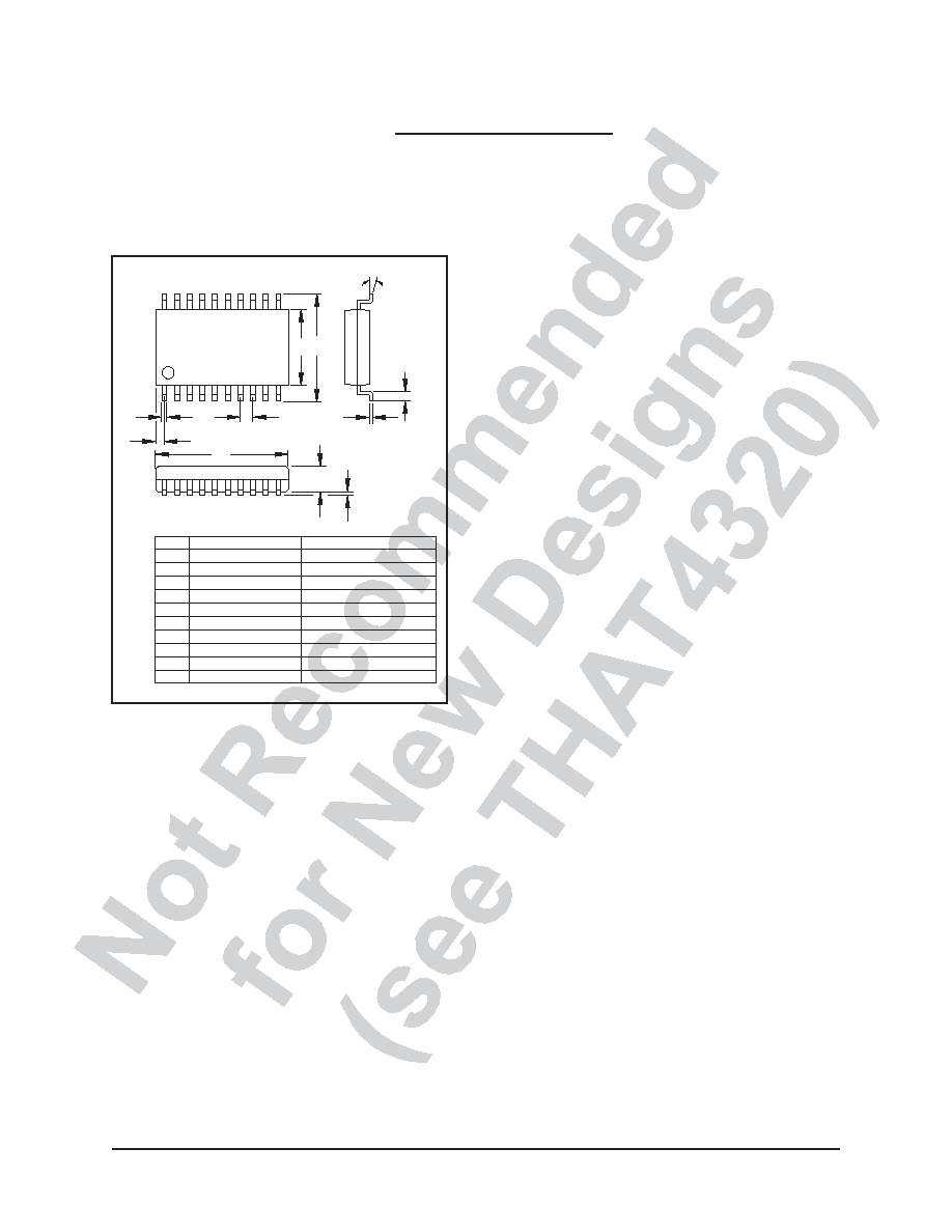
Package Information
The THAT 4311 is available in a 20-pin surface
mount package. The package dimensions are shown
in Fig 20 while the pinout is given in Table 1.
THAT Corporation; 45 Sumner Street; Milford, Massachusetts 01757-1656; USA
Tel: +1 508 478 9200; Fax: +1 508 478 0990; Web: www.thatcorp.com
Page 12
Low-voltage, Low-power Analog Engine
ģ
Dynamics Processor
A
D
1
B C
E
I
J
0-10ļ
G
H
F
Item
Millimeters
Inches
A
10.0 Ī 0.3
0.394 Ī 0.012
B
5.0 Ī 0.2
0.197 Ī 0.008
C
6.8 Ī 0.4
0.268 Ī 0.016
D
0.35 Ī 0.1
0.014 Ī 0.004
E
0.95
0.037
F
0.87 MAX
0.034 MAX
G
1.6 Ī 0.015
0.063 Ī 0.006
H
0.15 Ī 0.1
0.006 Ī 0.004
I
0.5 Ī 0.2
0.02 Ī 0.008
J
0.15 +0.1 -0.05
0.006 +0.004 -0.002
Figure 20. -S (DMP20 surface mount) package drawing